Comment by ElijahLynn
8 days ago
Wow, I wish we could post pictures to HN. That chip is HUGE!!!!
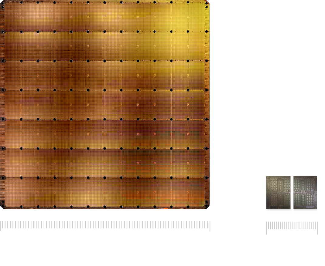
The WSE-3 is the largest AI chip ever built, measuring 46,255 mm² and containing 4 trillion transistors. It delivers 125 petaflops of AI compute through 900,000 AI-optimized cores — 19× more transistors and 28× more compute than the NVIDIA B200.
From https://www.cerebras.ai/chip:
https://cdn.sanity.io/images/e4qjo92p/production/78c94c67be9...
https://cdn.sanity.io/images/e4qjo92p/production/f552d23b565...
To be clear: that's the thousandths separator, not the Nordic decimal. It's the size of a cat, not the size of a thumbnail.
*thousands, not thousandths, right?
The correct number is fourty six thousand, two hundred and fifty five square mm.
Whoa, I just realized that the comma is the thousands separator when writing out the number in English words.
or about 0.23 furlongs
1 reply →
This is why space is the only acceptable thousands/grouping separator (a non-breaking space when possible). Avoids any confusion.
Space is also confusing! Then it looks like two separate numbers.
Underscore (_) is already used as a decimal separator in programming languages and Mathematics should just adopt it, IMO.
9 replies →
The problem is our primitive text representation online. The formatting should be localized but there’s not a number type I can easily insert inline in a text box.
46_255
Thanks, I was acutally wondering how would someone even manage to make that big a chip.
It's a whole wafer. Basically all chips are made on wafers that big, but normally it's a lot of different chips, you cut the wafer into small chips and throw the bad ones away.
Cerebras has other ways of marking the defects so they don't affect things.
Wow, I'm staggered, thanks for sharing
I was under the impression that often times chip manufacture at the top of the lines failed to be manufactured perfectly to spec and those with say, a core that was a bit under spec or which were missing a core would be down clocked or whatever and sold as the next in line chip.
Is that not a thing anymore? Or would a chip like this maybe be so specialized that you'd use say a generation earners transistor width and thus have more certainty of a successful cast?
Or does a chip this size just naturally ebb around 900,000 cores and that's not always the exact count?
20kwh! Wow! 900,000 cores. 125 teraflops of compute. Very neat
Designing to tolerate the defects is well trodden territory. You just expect some rate of defects and have a way of disabling failing blocks.
So you shoot for 10% more cores and disable failing cores?
3 replies →
IIRC, a lot of design went into making it so that you can disable parts of this chip selectively.
Why is the CEO some shady guy? though https://daloopa.com/blog/analyst-pov/cerebras-ipo-red-flags-...
"AI" always has some sleazy person behind it for some reason
You need the sleazy person because you need a shit-ton of money.
I have "shady CEO that doesn't give back to his country or community" fatigue
I sent this to someone I know knowledgeable about this type of thing, here’s what he had to say, sharing because I thought it was interesting:
Pretty cool tech, silicon is very advanced. That said, this is how every wafer comes out of the fab. This process does not dice out individual chips but instead adds interonnects. I doubt they have 100% yield, but probably just don't connect that die. This type of setup is one of the reasons Apple's M series chips are so effective. Their CPU/GPU/RAM are all on one die/directly interconnected instead of going through some motherboard based connector. I think Apple doesn't have them all go through the same process so those are connected via a different process but same layed on silicon direct connection. This solves the problem data centers tend to have of tons of latency for the connections between processors. This is also similar to AMD's infinity fabric of their Zen architecture. It's cool how all of these technologies build from another.
It's also all reliant on fab from TSMC who did the heavy lifting is making the process a reality
There have been discussions about this chip here in the past. Maybe not that particular one but previous versions of it. The whole server if I remember correctly eats some 20KWs of power.
A first-gen Oxide Computer rack puts out max 15 kW of power, and they manage to do that with air cooling. The liquid-cooled AI racks being used today for training and inference workloads almost certainly have far higher power output than that.
(Bringing liquid cooling to the racks likely has to be one of the biggest challenges with this whole new HPC/AI datacenter infrastructure, so the fact that an aircooled rack can just sit in mostly any ordinary facility is a non-trivial advantage.)
> The liquid-cooled AI racks being used today for training and inference workloads almost certainly have far higher power output than that.
75kW is a sane "default baseline" and you can find plenty of deployments at 130kW.
There's talk of pushing to 240kW and beyond...
> Bringing liquid cooling to the racks likely has to be one of the biggest challenges with this whole new HPC/AI
Are you sure about that? HPC has had full rack liquid cooling for a long time now.
The primary challenge with the current generation is the unusual increase of power density in racks. This necessitates upgrades in capacity, notably getting 10-20 kWh of heat away from few Us is generally though but if done can increase density.
1 reply →
Well for some. Google has been using liquid cooling to racks for decades.
That’s wild. That’s like running 15 indoor heaters at the same time.
20KW? Wow. That's a lot of power. Is that figure per hour?
What do you mean by "per hour"?
Watt is a measure of power, that is a rate: Joule/second, [energy/time]
> The watt (symbol: W) is the unit of power or radiant flux in the International System of Units (SI), equal to 1 joule per second or 1 kg⋅m2⋅s−3.[1][2][3] It is used to quantify the rate of energy transfer.
https://en.wikipedia.org/wiki/Watt
If you run it for an hour, yes.
12 replies →
It’s 20kW for as long as you can afford the power bill
3 replies →
20 kWh per hour
Maybe I'm silly, but why is this relevant to GPT-5.3-Codex-Spark?
It’s the chip they’re apparently running the model on.
> Codex-Spark runs on Cerebras’ Wafer Scale Engine 3 (opens in a new window)—a purpose-built AI accelerator for high-speed inference giving Codex a latency-first serving tier. We partnered with Cerebras to add this low-latency path to the same production serving stack as the rest of our fleet, so it works seamlessly across Codex and sets us up to support future models.
https://www.cerebras.ai/chip
That's what it's running on. It's optimized for very high throughput using Cerebras' hardware which is uniquely capable of running LLMs at very, very high speeds.
for cerbras, can we call them chips? you're no longer breaking the wafer we should call them slabs
They're still slices of a silicon ingot.
Just like potato chips are slices from a potato.
Macrochips
>Wow, I wish we could post pictures to HN. That chip is HUGE!!!!
Using a waffer sized chip doesn't sound great from a cost perspective when compared to using many smaller chips for inference. Yield will be much lower and prices higher.
Nevertheless, the actual price might not be very high if Cerebras doesn't apply an Nvidia level tax.
> Yield will be much lower and prices higher.
That's an intentional trade-off in the name of latency. We're going to see a further bifurcation in inference use-cases in the next 12 months. I'm expecting this distinction to become prominent:
(A) Massively parallel (optimize for token/$)
(B) Serial low latency (optimize for token/s).
Users will switch between A and B depending on need.
Examples of (A):
- "Search this 1M line codebase for DRY violations subject to $spec."
An example of (B):
- "Diagnose this one specific bug."
- "Apply this diff".
(B) is used in funnels to unblock (A). (A) is optimized for cost and bandwidth, (B) is optimized for latency.
As I understand it the chip consists of a huge number of processing units, with a mesh network between them so to speak, and they can tolerate disabling a number of units by routing around them.
Speed will suffer, but it's not like a stuck pixel on an 8k display rendering the whole panel useless (to consumers).
Cerebras addresses this in a blog post: https://www.cerebras.ai/blog/100x-defect-tolerance-how-cereb...
Basically they use very small cores compared to competitors, so faults only affect small areas.
Is this actually beneficial than, say having a bunch of smaller ones communicating on a bus? Apart from space constraints that is.
It's a single wafer, not a single compute core. A familiar equivalent might be putting 192 cores in a single Epyc CPU (or, more to be more technically accurate, the group of cores in a single CCD) rather than trying to interconnect 192 separate single core CPUs externally with each other.
Yes, bandwidth within a chip is much higher than on a bus.
Is all of it one chip? Seems like a waffer with several at least?
Those are scribe lines where you usually would cut out chips which is why it resembles multiple chips. However, they work with TSMC to etch across them.
Wooshka.
I hope they've got good heat sinks... and I hope they've plugged into renewable energy feeds...
Fresh water and gas turbines, I'm afraid...
Nope! It's gas turbines
For now. And also largely because it's easier to get that up and running than the alternative.
Eventually, as we ramp up on domestic solar production, (and even if we get rid of solar tariffs for a short period of time maybe?), the numbers will make them switch to renewable energy.
[flagged]
Bigger != Better
I can imagine how terribly bad their yield must be. One little mistake and the whole "chip" is a goner.
They have a blog post called "100x Defect Tolerance: How Cerebras Solved the Yield Problem":
https://www.cerebras.ai/blog/100x-defect-tolerance-how-cereb...
One thing is really bothering me: they show these tiny cores, but in the wafer comparison image, they chose to show their full chip as a square bounded by the circle of the wafer. Even the prior GPU arch tiled into the arcs of the circle. What gives?